LTFN is equipped with 3 worldwide unique pilot lines and clean room facilities and develops cutting-edge technologies for the Digital Nanomanufacturing of OE devices and multiscale characterization.
Lab for Thin Films - Nanobiomaterials - Nanosystems - Nanometrology

ORGANIC & PRINTED ELECTRONICS
LTFN posseses a clean room environment for scientific research of 500m2, with a low level of contamination such as dust, airborne, aerosol particles, and chemical vapors. In general, a cleanroom has a controlled level of contamination that is specified by the number of particles per cubic meter at a specified particle size. In Organic Electronic device packaging for instance, the default classification is ISO 5 (or a class 1.000,000) cleanroom.


Large area R2R manufacturing of OPVs, OLEDs, Sensors, OFETs onto plastics, equipped with Ultra-fast Laser scribing and in-line metrology systems.
Gravure Printing
R2R Gravure printing for high-throughput, high-quality printing with high resolution for manufacturing printed electronics.
Slot-Die Printing
R2R Slot Die coating provides smooth layers with homogeneous thickness in web direction and cross-direction and it can enable patterning of continues stripes of functional materials for organic electronic devices.
Inkjet Printing
R2R Inkjet printing allows direct patterning of all the layers, offering full freedom of design without the use of masks or structuring by hardware.
Screen Printing
R2R Screen printing allows the formation of a very thick wet layer and thereby also very thick dry films, which can be useful for printed electrodes where high conductivity is needed.
Laser Patterning
R2R Laser patterning enables the P1-P3 serial integration of flexible organic thin-film solar cells on polymer substrates, thus allowing new approaches to the module design.
Encapsulation Module
Encapsulation System equipped with 2 rolls for the lamination of High Barrier Films onto Flexible Electronic Devices. R2R Encapsulation takes place in the Lamination/Delamination Station, where R2R produced devices can be protected with high barrier films from oxygen and moisture.
Raman Spectroscopy
In-line Ellipsometry |
 |
LTFN excellence covers a wide spectrum of printing techniques (S2S Gravure, Slot-Die, Inkjet, etc.) for the Digital fabrication of Organic Electronics and Bioelectronics nanomaterials, devices and systems.
S2S Gravure PrintingPrinting using a sheet-to-sheet (S2S) lab scale gravure printing proofer for the optimization of layers for the fabrication of flexible organic electronic devices by a versatile and scalable gravure printing process. |
 |
Slot-Die mini Roll Coater
A compact slot-die coater and flexographic printing unit for flexible substrates. It is capable of coating without the operator having to touch the coated layers, while mimicking roll-to-roll coating conditions.
Inkjet PrintingA bench-top precision digital deposition system with versatile capability for high precision jetting of functional fluids on any type of surface. The system provides an easy-to-use, cost-effective tool to quickly develop and test processes and prototypes. |
 |

Hybrid printing and vacuum technologies for OE devices with encapsulation technologies and solar simulator system.
S2S Lamination System for the Encapsulation of Organic Electronic Devices in room or higher temperatures. Organic Electronic Devices are laminated in the S2S Encapsulated System under pressure at room or higher temperature conditions in various speeds.
Scalable OVPD Pilot Line equipped with in-situ optical metrology systems (Raman Spectroscopy, Spectroscopic Ellipsometry) for high precision fabrication of OPVs, OLEDs and sensors.
OVPD is an innovative technology for thin-film deposition of organic small molecules based on the gas phase transport principle for the production of Organic Solar Cells (OSCs), Organic Light Emitting Diodes (OLEDs) and flexible electronics. In addition, the introduction of in-line Spectroscopic Ellipsometry (SE) and Raman Spectroscopy (RS) at OVPD Cluster forms a unique combination for the production of optimized organic electronic devices.
|
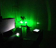
High energy laser systems for ultra fast processes (laser ablation, laser annealing, patterning etc.) for fabrication and functionalization of novel nanomaterials and nanoparticles. A ns pulsed Nd:YAG high energy laser system with multiple harmonics (1064, 532, 355,266, 213nm) for off line experiments. |
 |
Upcoming Events
Recent News
High Technology and Greek Innovation Transforming the Future of Green Energy (in Greek)
Agrivoltaics Event at Agrotica - March 14 (in Greek)
Presentation of the Flex2Energy and COPE-Nano projects at LOPEC 2026 in Munich (in Greek)
Two Flagship Projects of the European Green Industry at LOPEC 2026 (in Greek)
PRO Flextronics Feb 2026: OET - OPV as a Key Enabler for Smart Living and Mobility Applications
